

RF PCB affect wireless communication
Radio Frequency (RF) Printed Circuit Boards (PCBs) are integral to the functioning of wireless communication systems. These systems rely on high-frequency signals to transmit and receive data across various devices, from mobile phones and Wi-Fi routers to satellite systems and radar equipment. The RF PCB plays a critical role in ensuring that these systems perform effectively and with minimal interference. The design and performance of an RF PCB directly impact key aspects of wireless communication, such as signal strength, clarity, range, and reliability. Several factors within the RF PCB design influence how well wireless communication systems operate, including the layout, material selection, power handling, and noise management.
One of the most significant ways an RF PCB affects wireless communication is through signal integrity. The primary function of an RF PCB is to route and manage high-frequency signals, which are used to carry data in wireless communication systems. If the PCB is poorly designed, the signals can experience distortion, attenuation, or reflection, leading to poor data transmission or even total signal loss. A well-designed RF PCB minimizes these issues by ensuring that the signal traces have consistent impedance, preventing signal reflections and ensuring that the signals remain strong and clear as they travel through the system. By optimizing trace lengths and widths, minimizing signal path interference, and ensuring proper impedance matching, RF PCBs maintain high signal integrity, which is critical for reliable wireless communication.
Noise reduction is another critical factor influenced by the RF PCB design. Wireless communication systems often operate in environments with high levels of electromagnetic interference (EMI) from external sources, such as power lines, other electronic devices, or even atmospheric conditions. If an RF PCB does not adequately manage noise, the signals can become contaminated with unwanted interference, which can degrade performance and lead to poor communication quality. rf pcb use several techniques to reduce noise, such as incorporating ground planes, shielding, and filtering components. A continuous ground plane, for example, helps to reduce EMI by providing a low-resistance path for the return currents, while shielding prevents external interference from reaching sensitive signal traces. Capacitors and inductors are often used to filter out high-frequency noise, allowing only the desired signals to pass through.
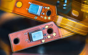
How does an RF PCB affect wireless communication?
The material selection of the RF PCB is another factor that directly influences wireless communication. RF PCBs must be made from materials that can handle high-frequency signals with minimal loss and attenuation. Materials such as Teflon (PTFE), ceramic composites, or epoxy glass laminates are commonly used in RF PCBs because they offer low dielectric loss, high thermal stability, and consistent electrical properties. These materials help to preserve the strength and quality of RF signals as they pass through the PCB, ensuring that the wireless communication system functions efficiently over long distances and at high frequencies. The choice of materials also affects the overall power handling capacity and thermal performance of the PCB, which are important for preventing overheating and ensuring that the system remains stable under high load conditions.
The power handling capacity of an RF PCB is another important consideration in wireless communication. Wireless communication systems often need to transmit signals over long distances or through challenging environments, which requires the system to handle higher power levels. The RF PCB must be designed to accommodate the power levels required without causing excessive heat buildup or signal degradation. Heat dissipation techniques, such as using heat sinks, thermal vias, and large ground planes, are often incorporated into the design to manage heat generated by high-power signals. By properly managing power handling and thermal performance, RF PCBs help maintain the reliability and stability of wireless communication systems, preventing failures or interruptions due to overheating.
Finally, component integration and miniaturization on RF PCBs also contribute to the performance of wireless communication systems. The trend toward smaller, more compact devices in modern wireless technology demands that the RF PCB be able to integrate multiple functions within a limited space. By efficiently integrating components like filters, amplifiers, oscillators, and antennas, RF PCBs help reduce the size of wireless communication devices without sacrificing performance. Advanced packaging techniques and multi-layer designs allow engineers to integrate more components into a single PCB, optimizing the space and improving overall system performance.
In conclusion, an RF PCB plays a pivotal role in the success of wireless communication systems by maintaining signal integrity, reducing noise, ensuring proper power handling, and supporting efficient component integration. The design, material selection, and construction of the PCB directly affect the performance, reliability, and range of wireless devices. By addressing these factors, RF PCBs help ensure that wireless communication systems operate effectively, providing users with clear, reliable, and high-performance communication across various platforms.